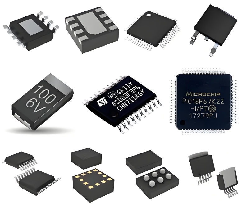
Infineon IRS4427STRPBF Low-Side Gate Driver IC: Datasheet, Pinout, and Application Circuit Design
The Infineon IRS4427STRPBF is a robust and high-performance low-side gate driver IC designed to efficiently control the switching of power MOSFETs and IGBTs. As a critical component in modern power electronics, it serves as an essential interface between a low-power controller (like a microcontroller or PWM IC) and the high-power switch. Its primary function is to amplify a logic-level signal into a high-current, high-voltage output capable of rapidly charging and discharging the capacitive gate of a power transistor, thereby minimizing switching losses and improving overall system efficiency.
This driver is part of Infineon's extensive portfolio and is housed in a compact SOIC-8 package, making it suitable for a wide array of applications, including switch-mode power supplies (SMPS), motor control systems, DC-DC converters, and lighting ballasts.
Key Datasheet Specifications and Features
The IRS4427STRPBF's datasheet reveals a component engineered for speed, robustness, and protection. Key electrical characteristics include:
High Output Current: Capable of sourcing +1.4A and sinking -1.8A peak currents, enabling very fast switching transitions.
Wide Operating Voltage Range (VB): From 10V to 20V, providing flexibility in designing the gate drive voltage.
CMOS/LSTTL Compatible Inputs: The input pin is compatible with 3.3V and 5V logic signals, ensuring easy connection to modern microcontrollers without additional level-shifting circuitry.
Matched Propagation Delay Times: Typical delay is 85ns, which ensures precise timing control critical for high-frequency operation.
Undervoltage Lockout (UVLO): A crucial protection feature that keeps the output low if the supply voltage (VCC) is below a specified threshold (typically ~8.7V), preventing the power switch from operating in a high-resistance linear mode, which could lead to excessive heating and failure.
High Noise Immunity: The input stage is designed with Schmitt-trigger characteristics, providing excellent noise rejection and preventing false triggering from spurious signals.
Pinout Configuration (SOIC-8 Package)
Understanding the pinout is fundamental for correct PCB layout:
1. VCC: Pin 1. This is the positive supply voltage pin for the driver IC's internal circuitry. A high-quality, locally decoupled capacitor is mandatory here.
2. IN: Pin 2. The logic input pin. This pin receives the PWM control signal from the microcontroller or controller IC.
3. GND: Pin 3. The ground reference for the IC. This must be connected to the system ground plane with low impedance.
4. NC: Pins 4 and 5. No Connection. These pins are not internally connected.

5. OUT: Pin 6. The gate driver output. This pin is connected directly to the gate of the external MOSFET or IGBT through a small gate resistor.
6. VB: Pin 7. This pin is internally connected to VCC in the IRS4427. For some drivers, this is a bootstrap supply, but here it is tied to the main supply.
7. VS: Pin 8. This pin is internally connected to GND in the IRS4427, serving as the low-side reference for the output stage.
Typical Application Circuit Design
A basic application circuit for driving a low-side MOSFET is straightforward but requires careful attention to component selection and layout:
1. Power Decoupling: Place a ceramic capacitor (e.g., 100nF) as close as possible between the VCC (Pin 1) and GND (Pin 3) pins to filter high-frequency noise. A larger bulk electrolytic or tantalum capacitor (e.g., 10µF) should be placed nearby for stabilizing the supply.
2. Input Resistor (Optional): A small series resistor (e.g., 10-100Ω) on the IN pin can help dampen any ringing caused by lead inductance.
3. Gate Resistor (RG): A critical component placed in series between the driver's OUT (Pin 6) and the MOSFET gate. This resistor controls the switch's rise and fall times, trading off between switching speed (efficiency) and overshoot/ringing (EMI). A value between 5Ω to 100Ω is typical and should be determined experimentally.
4. Gate-to-Source Resistor (RGS): A high-value resistor (e.g., 10kΩ to 100kΩ) connected directly between the MOSFET's gate and source terminals is often used to ensure stable turn-off by providing a discharge path for any leakage current, preventing accidental turn-on.
5. Load: The drain of the MOSFET is connected to the high-side load (e.g., a motor winding, transformer, or LED string), while the source is connected directly to ground.
ICGOODFIND Summary
The Infineon IRS4427STRPBF is a highly reliable and efficient solution for low-side switching applications. Its strong drive current, integrated UVLO protection, and logic-level compatibility make it an excellent choice for designers seeking to improve the performance and robustness of their power conversion systems. Proper implementation, focusing on tight decoupling and careful gate resistor selection, is key to unlocking its full potential.
Keywords:
Gate Driver IC
Low-Side Switching
Undervoltage Lockout (UVLO)
MOSFET
Application Circuit
